nanofabrication icon no background

Core Nanofabrication

The Core Nanofabrication cleanrooms provide the ideal environment to produce high-quality devices. With an extensive range of equipment, they can support activities with a broad variety of materials including compound semiconductors, silicon, diamond and organic semiconductor materials from chips to small batches of wafers.

The cleanrooms offer a full range of routine fabrication capabilities including:

  • Mask-based photolithography (chips to 6” wafers)
  • Thermal and e-beam evaporation of metals
  • Dielectric deposition by PECVD and ALD
  • Dry etching of dielectrics, compound semiconductor materials and silicon
  • Metrology, inspection and testing
  • Cleaving, Sawing and die packaging

The Core Nanofabrication cleanrooms provide the ideal environment to produce high-quality devices. With an extensive range of equipment, they can support activities with a broad variety of materials including compound semiconductors, silicon, diamond and organic semiconductor materials from chips to small batches of wafers.

The cleanrooms offer a full range of routine fabrication capabilities including:

  • Mask-based photolithography (chips to 6” wafers)
  • Thermal and e-beam evaporation of metals
  • Dielectric deposition by PECVD and ALD
  • Dry etching of dielectrics, compound semiconductor materials and silicon
  • Metrology, inspection and testing
  • Cleaving, Sawing and die packaging.

  • Mask-based photolithography (chips to 6” wafers)
  • Thermal and e-beam evaporation of metals
  • Dielectric deposition by PECVD and ALD
  • Dry etching of dielectrics, compound semiconductor materials and silicon
  • Metrology, inspection and testing
  • Cleaving, Sawing and die packaging

Our Capabilities

Manual spin coaters, manual mask aligners, manual development for chips and small wafers up to 3” diameter 

Including hydrofluoric acid (HF) etches

Dielectrics, III-V materials, potentially silicon (mainly for photonics, mems)

Thermal, sputter, self-contained systems for deposition of thermal and beam evaporation. Deposition of single films and multilayer stacks of metal.

Including plasma-enhanced chemical vapor deposition (PECVD) using silicon nitride (SiNx) and silicon oxide (SiOx), and thermal atomic layer deposition (ALD).

Surface profiling (stylus; AFM), Dielectric thin film characterisation (ellipsometry), optical microscopy.

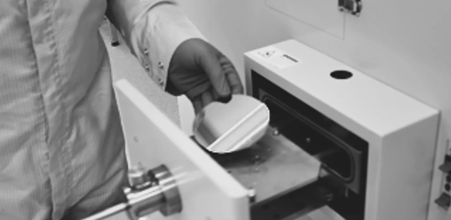
Wafer cleaving and sawing plus basic device packaging

Operating Modes

Service Mode

Enquire about this Facility

core-nano-1080x1920

If you are new to CORDE we would recommend contacting us via the form below to ensure we can help you with a detailed response. Or you can contact the Core Nanofabrication Facility Scientist directly at nanofab@phy.cam.ac.uk.