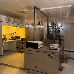
E-beam writer capable of patterning substrates of up to 200mm diameter with a resolution as high as 10nm to produce samples for a wide variety of academic and industrial users.
One of the fastest Gaussian Beam systems on the market, with a fast, arbitrary shape pattern generator of 100MHz.


If you are new to CORDE we would recommend contacting us via the form below to ensure we can help you with a detailed response. Or you can contact the E-beam Lithography Facility Scientist directly at ebeam@phy.cam.uk.
Vianez P. M. T., Jin Y., Moreno M., Anirban A. S., Anthore A., Tan W. K., Miao Q., Griffiths J. P., Farrer I., Ritchie D. A., Schofield A. J., Tsyplyatyev O. and Ford C. J. B
Observing separate spin and charge Fermi seas in a strongly correlated one-dimensional conductor,
In: Science Advances 2022, 8, eabm2781–1–9. doi: 10.1126/sciadv.abm2781
An electron is usually considered to have only one form of kinetic energy, but could it have more, for its spin and charge, by exciting other electrons? In one dimension (1D), the physics of interacting electrons is captured well at low energies by the Tomonaga-Luttinger model, yet little has been observed experimentally beyond this linear regime. Here, we report on measurements of many-body modes in 1D gated wires using tunneling spectroscopy. We observe two parabolic dispersions, indicative of separate Fermi seas at high energies, associated with spin and charge excitations, together with the emergence of two additional 1D “replica” modes that strengthen with decreasing wire length. The interaction strength is varied by changing the amount of 1D intersubband screening by more than 45%. Our findings not only demonstrate the existence of spin-charge separation in the whole energy band outside the low-energy limit of the Tomonaga-Luttinger model but also set a constraint on the validity of the newer nonlinear Tomonaga-Luttinger theory.
Fruhman J. M., Astier H. P. A. G., Ehrler B., Böhm M. L., Eyre L. F. L., Kidambi P. R., Sassi U., Fazio D. De, Griffiths J. P., Robson A. J., Robinson B. J., Hofmann S., Ferrari A. C. and Ford C. J. B.
In: Nature Communications 2021, 12, 4307. doi: https://doi.org/10.1038/s41467-021-24233-2
It is challenging for conventional top-down lithography to fabricate reproducible devices very close to atomic dimensions, whereas identical molecules and very similar nanoparticles can be made bottom-up in large quantities, and can be self-assembled on surfaces. The challenge is to fabricate electrical contacts to many such small objects at the same time, so that nanocrystals and molecules can be incorporated into conventional integrated circuits. Here, we report a scalable method for contacting a self-assembled monolayer of nanoparticles with a single layer of graphene. This produces single-electron effects, in the form of a Coulomb staircase, with a yield of 87 ± 13% in device areas ranging from < 800 nm 2 to 16 μm 2 , con- taining up to 650,000 nanoparticles. Our technique offers scalable assembly of ultra-high densities of functional particles or molecules that could be used in electronic integrated circuits, as memories, switches, sensors or thermoelectric generators.