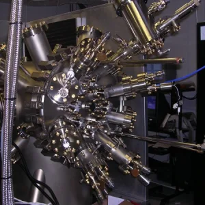
III-V (Arsinides) work is undertaken on our Veeco GEN III and Veeco modGEN II growth chambers on up to 3” substrates; the GEN III is UHV connected to a dedicated Veeco 620 system which allows for in-situ atomic hydrogen surface cleaning/preparation and secondary ion mass spectrometry (SIMS) characterisation.
The Topological Materials chamber is a PREVAC MBE dual chamber design, funded by the Royce Institute, that supports growth on up to 2” substrates. The main chamber allows epitaxial growth of Topological and related materials and is UHV connected to a secondary chamber that currently allows deposition of a range of metals.


If you are new to CORDE we would recommend contacting us via the form below to ensure we can help you with a detailed response. Or you can contact the Growth Facility Scientist directly at growth@phy.cam.uk.
Lev V. Levitin, Harriet van der Vliet, Terje Theisen, Stefanos Dimitriadis, Marijn Lucas, Antonio D. Corcoles, Ján Nyéki, Andrew J. Casey, Graham Creeth, Ian Farrer, David A. Ritchie, James T. Nicholls & John Saunders
Cooling low-dimensional electron systems into the microkelvin regime
In: Nature Communications, 13, Article number: 667 (2022). doi: 10.1038/s41467-022-28222-x
Two-dimensional electron gases (2DEGs) with high mobility, engineered in semiconductor heterostructures host a variety of ordered phases arising from strong correlations, which emerge at sufficiently low temperatures. The 2DEG can be further controlled by surface gates to create quasi-one dimensional systems, with potential spintronic applications. Here we address the long-standing challenge of cooling such electrons to below 1 mK, potentially important for identification of topological phases and spin correlated states. The 2DEG device was immersed in liquid 3He, cooled by the nuclear adiabatic demagnetization of copper. The temperature of the 2D electrons was inferred from the electronic noise in a gold wire, connected to the 2DEG by a metallic ohmic contact. With effective screening and filtering, we demonstrate a temperature of 0.9 ± 0.1 mK, with scope for significant further improvement. This platform is a key technological step, paving the way to observing new quantum phenomena, and developing new generations of nanoelectronic devices exploiting correlated electron states.
S N Holmes; C Chen; D A Ritchie; M Pepper
Variable range hopping conductivity in molecular beam epitaxial InSb
In: Journal of Physics D: Applied Physics, vol. 55 no. 46. doi: 10.1088/1361-6463/ac941c
A variable range hopping (VRH) transport mechanism can be induced in molecular beam epitaxial, n-type doped InSb wafers with focussed Ga+ ion beam damage. This technique allows areas of wafer to be selectively damaged and then subsequently processed into gated metal–insulator–semiconductor (MIS) devices where a disordered, two-dimensional (2D) device can be established. At high levels of damage (dose >1016 Ga+ ions cm−2) amorphous crystalline behavior results with activated conductivity characteristic of a three-dimensional system with VRH below 150 K. At lower doses (1014–1016 Ga+ ions cm−2) a thermally activated conductivity is induced at ∼0.9 K, characteristic of Mott phonon-assisted VRH. At 1 K the devices either conduct with conductivity >∼(e2/h) where e is the fundamental charge and h is Planck’s constant, or are thermally activated depending on the dose level. The lightly damaged devices show weak antilocalization signals with conductivity characteristic of a 2D electronic system. As the Ga+ dose increases, the measured phase coherence length reduces from ∼500 nm to ∼100 nm. This provides a region of VRH transport where phase-coherent transport processes can be studied in the hopping regime with the dimensionality controlled by a gate voltage in an MIS-device.